
PCBA one-stop Solutions
PCBA one-stop design and production solutions for various industry applications.
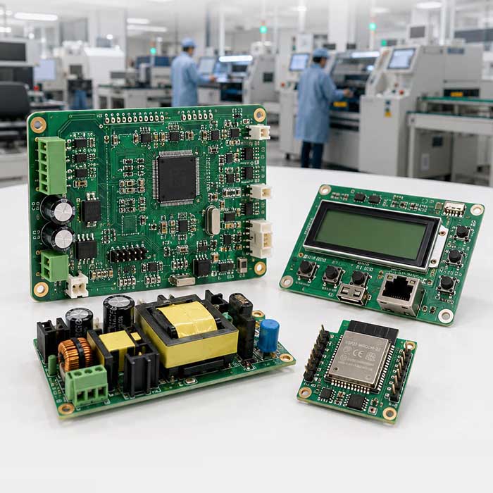
From project evaluation to finished product delivery
We can assist in the assessment at different project stages.
1. Complete production files available
The Gerber, BOM, coordinates and assembly drawings are all complete, allowing for direct evaluation of board manufacturing and mounting.
2. Only physical samples are available
Supports reverse engineering analysis, component identification, BOM organization, PCB replication and schematic reconstruction.
3. Only functional requirements
First, sort out the functional, interface, power supply and structural requirements, and then evaluate the development approach of the solution.
PCBA one-stop service process
01.
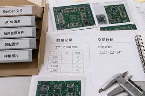
File and requirement confirmation
Receive project data, confirm quantity, delivery date, process and testing requirements.
02.
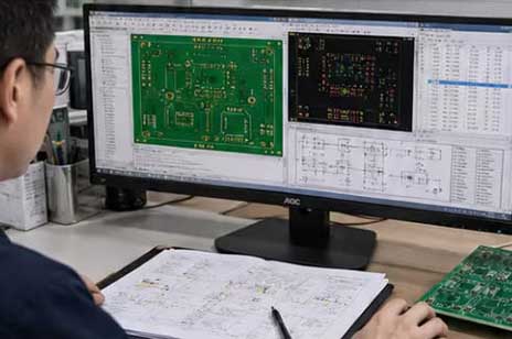
Engineering review and production confirmation
Before production, verify the consistency of the data to identify packaging, orientation and assembly risks in advance.
03.
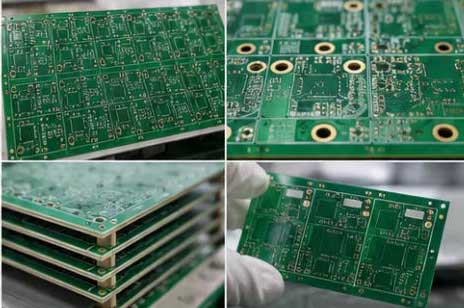
PCB manufacturing
Arrange the PCB production according to the engineering data, confirm the type of board, number of layers, board thickness and surface treatment.
04.
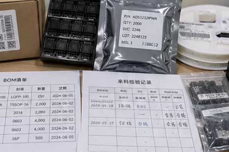
Procurement of components
Arrange material procurement based on the BOM, and verify the model, packaging, quantity and delivery date.
05.
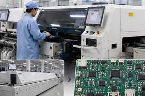
SMT assembly
Complete solder paste printing, surface mount technology (SMT) placement and reflow soldering to form SMT semi-finished products.
06.
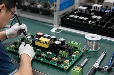
DIP and manual welding
Complete the welding and assembly of plug-in devices, connectors and special components.
07.
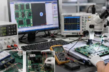
Detection, burning and functional testing
Conduct appearance inspection, program burning, power-on and functional testing according to project requirements
08.
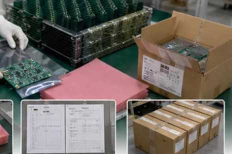
Cleaning, packaging and delivery
Complete cleaning, packaging and shipping preparations, and deliver the finished products as required